Overview
| Optical trapping |
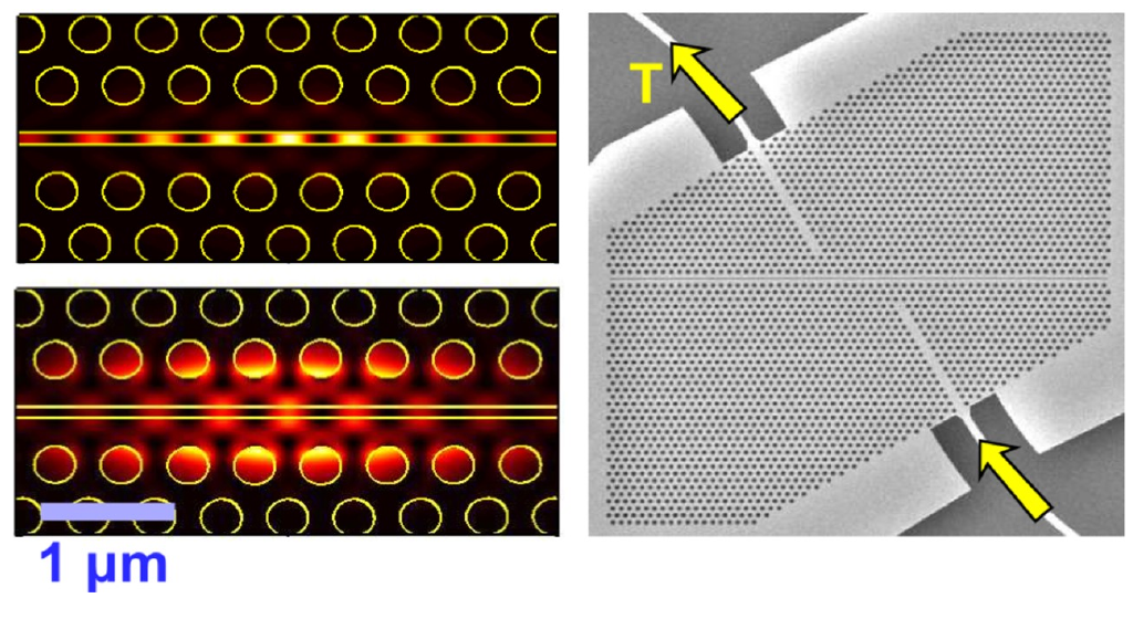 |
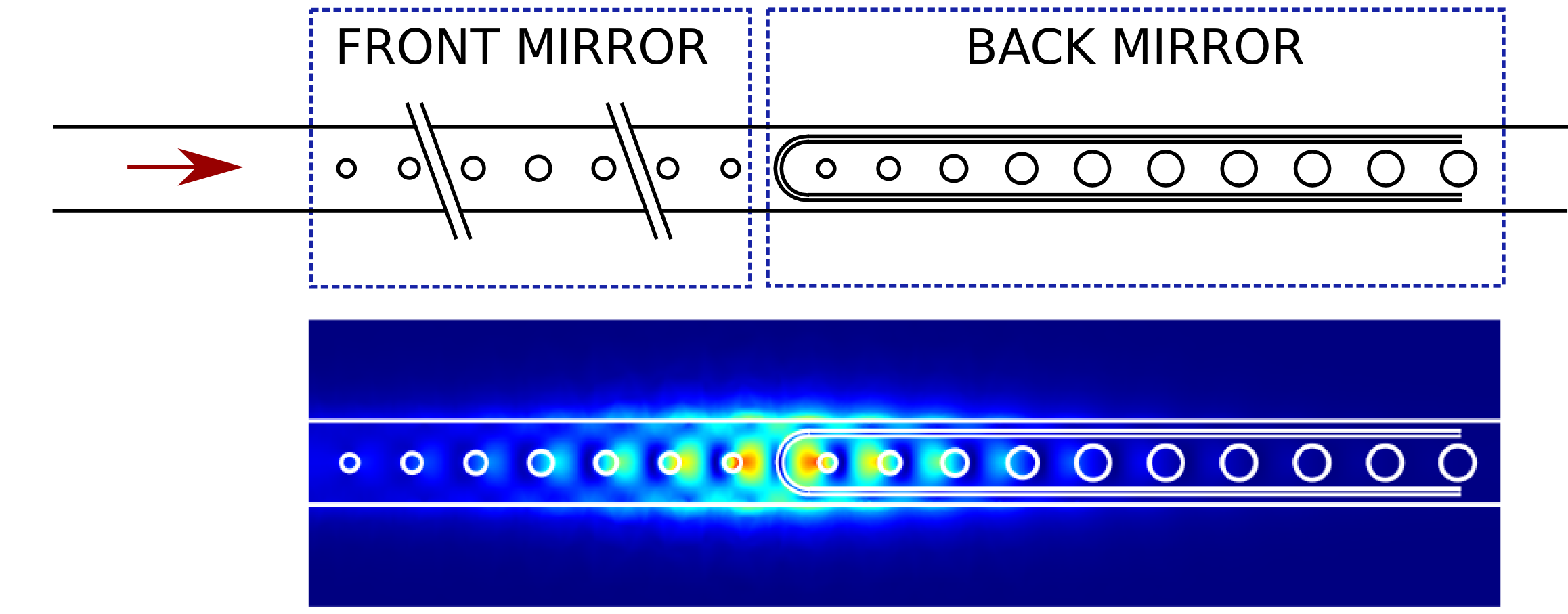
Our group is broadly interested in developing and using nanometre scale "engineering" techniques and tools to produce novel optical/photonic structures and devices that can be used for scientific exploration and potentially form the basis of new nanotechnologies. Most of the work is directly or indirectly concerned with artificially enhancing the effective strength of the interaction between light (photons) and matter (electrons). Some of the materials of interest include semiconductor and metallic nanoparticles, dye molecules or polymers. We typically employ 3 dimensional (3D) texturing of semiconductor or metallic materials in order to locally enhance the electric field of light beams at the location of the materials of interest.
| Superconducting Single Photon Detector |
 |
Why is this important/useful? Quite generally, the stronger the interaction strength between a light field and some material medium, the lower is the optical power required to induce some measurable response in the material. We engineer enhanced light-matter interactions for applications including:
- Optical trapping
- Superconducting Single Photon Detection
- Single Photon Sources
We are part of the Quantum Materials Institute at UBC, and we have both an in-house scanning electron microscope (SEM) for imaging and electron beam lithography and a cleanroom nanofabrication facility on-site. We also use the JEOL JBX-6300FS Electron Beam Lithography System at the University of Washington to fabricate silicon-on-insulator photonic circuits. The main optics labs contain a host of spectroscopy tools, mostly devoted to infrared wavelengths. We have access to a number of electrodynamic design and layout tools including Lumerical Solutions FDTD software, COMSOL, Mentor Graphics etc., some of which is provided with support from the Canadian Microelectronics Corporation (CMC).